
Dispersion Parameters and Electrical Characterization of Cd₁₋ₓCuₓS Thin Films Deposited by Using AACVD Technique
DOI:
https://doi.org/10.22401/Keywords:
Urbach Energy, Dispersion Parameters, SEM-EDX, AACVDAbstract
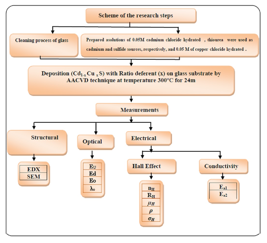
In this research, an aerosol-assisted chemical vapor deposition (AACVD) was successfully employed to synthesize Cd₁₋ₓCuₓS (0 ≤ x ≤ 1) semiconductor thin films. The structural, morphological, and optical properties of the deposited films were systematically investigated as a function of copper concentration using energy-dispersive X-ray spectroscopy (EDX), scanning electron microscopy (SEM), and UV-Vis spectroscopy. The results demonstrated that the optical behavior of the films is strongly influenced by Cu incorporation. Specifically, an increase in CdS fraction resulted in a decrease in the Urbach energy, whereas the activation energy exhibited a progressive increase with higher CuS content.
References
[1] Wondmagegn, W.; Marandi, M.; Saievar-Iranizad, E.; Taghavinia, N.; Liu, B.; Sun, H. D.; "CdS thin film transistor for inverter and operational amplifier circuit applications". Microelectron. Eng., 157: 64–70, 2016.
[2] Molaei, M.; Marandi, M.; Saievar-Iranizad, E.; Taghavinia, N.; Liu, B.; Sun, H. D.; Sun, X. W.; "Near-white emitting QD-LED based on hydrophilic CdS nanocrystals". J. Lumin., 132: 467–473, 2012.
[3] Li, P.; Wang, Y.; Zhang, Y.; Wang, X.; "TiO₂ activity enhancement through synergistic effect of photons localization of photonic crystals and the sensitization of CdS quantum dots". Photon. Nanostruct.-Fundam. Appl., 23: 12–20, 2017.
[4] Wang, F.; Liang, L.; Chen, K.; Sun, J.; "CO₂ induced template approach to fabricate the porous C/CdS visible photocatalyst with superior activity and stability". J. Mol. Catal. A Chem., 425: 76–85, 2016.
[5] Sharma, A.; Kumar, R.; Bhattacharyya, B.; Husale, S.; "Hot electron induced NIR detection in CdS films," Sci. Rep., 6: 22939, 2016.
[6] Adem, K.; "Electronic Properties of PbTe/Si Heterojunction". Al-Nahrain J. Sci., 15(4): 129–133, 2012.
[7] Camacho-Espinosa, E.; Rejón, V.; Hernández-Rodríguez, E.; Mis-Fernández, R.; "CHClF₂ gas mixtures to activate all-sputtered CdS/CdTe solar cells". Sol. Energy, 144: 729–734, 2017.
[8] Ghosh, B.; Das, M.; Banerjee, P.; Das, S.; "Fabrication of vacuum-evaporated SnS/CdS heterojunction for PV applications". Sol. Energy Mater. Sol. Cells, 92: 1099–1104, 2008.
[9] Hincapié-Zapata, J. M.; Castrillón-González, E. Y.; Cruz-Muñoz, B.; Medina-Barreto, M. H.; Dorantes-Rodríguez, R. J.; "Instrumentation and control of an aerosol-assisted chemical vapor deposition system (AACVD) ". Dyna, 86(210): 52–57, 2019.
[10] Choy, K. L.; "Chemical vapour deposition of coatings". Prog. Mater. Sci., 48(2): 57–170, 2003.
[11] Monárrez-Cordero, B. E.; Amézaga-Madrid, P.; Sáenz-Trevizo, A.; Pizá-Ruiz, P.; Antúnez-Flores, W.; Miki-Yoshida, M.; "Synthesis and characterization of composite Fe-Ti oxides nanoparticles with high surface area obtained via AACVD". Ceram. Int., 44(6): 6990–6996, 2018.
[12] Ahmed, M.; Bakry, A.; Dalir, H.; Shaaban, E. R.; "Copper effect on cadmium sulfide thin films for spintronics: microstructures, morphological, photoluminescence and magnetic properties". J. Mater. Sci. Mater. Electron., 19(11): 785–792, 2022.
[13] Goldstein, J. I.; Newbury, D. E.; Michael, J. R.; Ritchie, N. W. M.; Scott, J. H. J.; Joy, D. C.; "Scanning electron microscopy and X-ray microanalysis". In Scanning Electron Microscopy and X-ray Microanalysis, 4th ed.; Springer, New York, USA, pp. 1–832, 2018.
[14] Reimer, L.; "Physics of image formation in scanning electron microscopy". In Scanning Electron Microscopy: Physics of Image Formation and Microanalysis, 2nd ed.; Springer, Berlin, Germany, pp. 1–435, 1998.
[15] Hassan, N. B.; "Dispersion Parameters and Morphology of Chemical Spray Pyrolysis Deposited Fe₂O₃ Thin Films Prepared at Different Thickness". Indian J. Appl. Res., 3(6): 449–452, 2011.
[16] El-Zaiat, S. Y.; El-Den, M. B.; El-Kameesy, S. U.; El-Gammam, Y. A.; "Spectral dispersion of linear optical properties for Sm₂O₃ doped B₂O₃–PbO–Al₂O₃ glasses". Opt. Laser Technol., 44(5): 1270–1276, 2012.
[17] Kamruzzaman, M.; Runa, T.; Podder, J.; Anowar, M. G. M.; "Synthesis and Characterization of Cd₁₋ₓCuₓS Thin Films Prepared Using the Spray Pyrolysis Technique". Semicond. Sci. Technol., 27(3): 035017, 2012.
[18] Farag, A. A.; Ibrahim, M. A.; Ismail, F. M.; "Electrical and optical properties of sprayed CdS thin films". Chalcogenide Lett., 6(12): 267–276, 2009.
[19] Diliegros-Godines, C. J.; Lombardero-Juárez, D. I.; Machorro-Mejía, R.; González, R. S.; Pal, M.; "Electrical properties and spectroscopic ellipsometry studies of covellite CuS thin films deposited from non-ammoniacal chemical bath". Opt. Mater., 91: 147–154, 2019.
Downloads
Published
Issue
Section
License
Copyright (c) 2026 Zaid Mohammed Jasim, Nahida B. Hasan, Mohsin K. Al-khaykanee

This work is licensed under a Creative Commons Attribution 4.0 International License.

.jpg)